A joint research team in Japan has developed a “single-seed cast method,” a new casting method making it possible to grow high-quality mono silicon at low cost. New casting method may facilitate the return of a market-competitive solar cell industry.
Floating Solar Panels: A Viable Solution?
by

Hydro Power | Photovoltaic Cells | Solar PowerSince 2011, French Company Ciel & Terre has been developing large-scale floating solar solutions. Their innovative Hydrelio Floating PV system allows standard PV panels to be installed on large bodies of water such as: drinking water reservoirs, quarry lakes, irrigation canals, remediation and tailing ponds, and hydro electric dam reservoirs. This simple and affordable alternative […]
Switchable material could enable new memory chips
by

Small voltage can flip thin film between two crystal states — one metallic, one semiconducting — new research indicates. The research involves a thin-film material called a strontium cobaltite, or SrCoOx.
Visualizing atoms of perovskite crystals
by

Researchers conduct the first atomic resolution study of perovskites used in next generation solar cells.
3D Printed Solar Energy Trees
by

Energy Inventions | Future Technology | Photovoltaic Cells | Solar PowerHow would nature do it? Researchers at the VTT Technical Research Centre of Finland may be discovering the answer, thanks to advancing solar and 3D printing technologies. They have developed some very decorative prototypes of what they are calling “energy harvesting trees”. The tiny leaves generate and store solar energy and can be used to […]
Solar water splitting: Putting an extra ‘eye’ on surface reactions that store sunlight as fuel
by

Water-splitting cells absorb sunlight and produce fuel. Creating such cells means pairing a material to absorb sunlight and generate electrons with the one that uses those electrons to produce fuel. Scientists introduced a novel way to study the flow of electrons where the materials meet.
Breakthrough to the development of energy-saving devices for the next generation
by
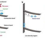
Researchers have succeeded in visualizing changes in defect density on the surface of GaN through the laser terahertz emission microscope (LTEM) which measures THz waves generated by laser emission. The discovery shows that LTEM is useful as a new method for evaluating the quality of wide-gap semiconductors and it is also expected that LTEM will bring a breakthrough in the development of next-generation optical devices, super high frequency devices, and energy devices.